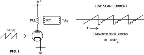
Postwar Television Television Line Output Stages and the Evolution of the Damper Diode or "Energy Recovery Diode"By Dr. Hugo Holden The circuits have been reduced to their basic forms without linearity or width controls so as to show their basic configuration. Coupling the yoke to the line output tube by a transformer is shown in Fig 1. At flyback the tube is cut-off and the magnetic field in the transformer and yoke collapses and resonates due to the self-inductance and distributed capacitance of these structures. There are oscillatory voltages and currents representing relatively undamped oscillations. These oscillations, which are visible in the scanning raster, decay away, and become damped out when the line output tube is again driven into conduction by the drive voltage. These oscillations must be eliminated for a satisfactory scanning raster. 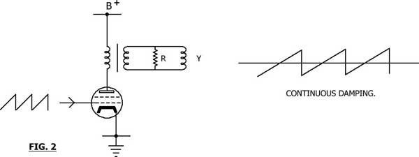
Fig 2 shows resistive damping. In this case the damping occurs across the entire duration of the sawtooth current scanning waveform on both the positive and negative excursions of current, so it can be called bidirectional damping. This is wasteful of energy, lengthens the flyback period, and reduces the opportunity to utilize the positive going high voltage spikes generated at the line output tube's anode, or via an overwind coil to generate EHT. 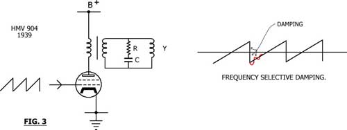
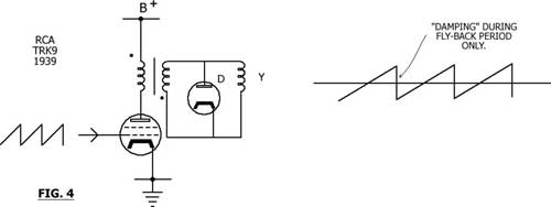
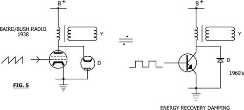
Fig 3 shows an improvement to resistive damping. This technique is used in the HMV Marconi 904(1939). The RC network is frequency selective, damping the parts of the waveform with the highest rates of change. This reduces the oscillations of currents (shown in red) however, because the flyback period contains high frequency (Fourier) components, this is also damped. Again this wastes energy and lengthens the flyback period. Fig 4 Shows what might appear to be the introduction of an efficiency diode in the RCA TRK9 (and TRK 12) but is in fact, not. This circuit has the damper conducting only over flyback time alone, and is really a spike suppressor. A true efficiency diode conducts during the active scan time on the left hand side of the scanning raster and recovers energy from the magnetic field of the yoke and line output transformer. The recovered energy is stored in the magnetic field at the end of scan time at the right side of the raster. The circuit of fig 4 damps the flyback voltage oscillations and absorbs energy when the output tube is cut off. This arrangement can't be used in a system to generate EHT from the flyback voltage spike. In 1938 the Baird/Bush TV and radio company in the United Kingdom were using the circuit shown in Fig 5: (Provided by Mr Victor Barker, AUSTRALIA) This is probably one of the first examples of energy recovery scanning. When the magnetic field in the line output transformer collapses, the diode conducts on the first negative half cycle of voltage on the diode's cathode, to produce a more linear rate of change of current. This damps the oscillations and also returns energy to the power supply. As can be seen this was the precursor of the typical transistorised line output stage that appeared in early transistor televisions in the early 1960's. 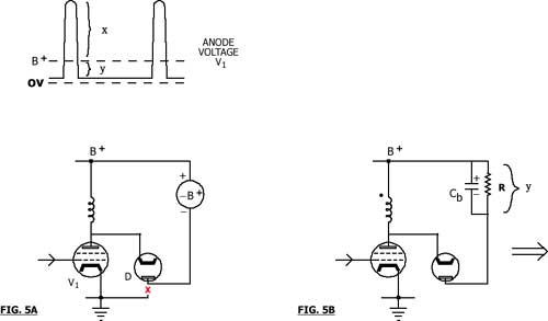
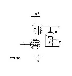
Returning to this later, let's look at this Bush circuit in the following three equivalents: Rather than returning the anode to ground (zero volts), it can be returned to B+ provided B+ is cancelled to zero volts (or close) by another "-B+" supply as seen in Fig 5A. This added supply can then be replaced with an RC network, as seen in Fig 5B, which charges to a value Y, say close to the value of B+ but in practice is a little less as the line opt tube anode voltage doesn't go completely to zero during active scan time. Then simply this diode and RC network is placed on a secondary winding, not the primary, and the position of the diode and RC network reversed as they're in a series circuit then you end up with the following seen in Fig 5C:
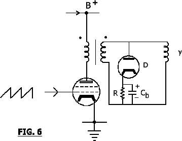
When the line output tube is cut-off at flyback, the first half cycle of voltage oscillation takes the damper anode negative (cutting it off during flyback). The damper anode has the opposite polarity to the anode of the line output tube. Then on the first positive half cycle of the voltage oscillations at the damper anode, the damper conducts. This damps the oscillations and results in a near linear scanning current, at the left side of the raster, as the magnetic field in the yoke and transformer now collapse in a controlled (damped) linear way toward zero. Before the current reaches zero however, the line output tube is driven into conduction and the process repeats. The circuit of the yoke and transformer represents an inductor with series resistance tuned by parallel distributed capacity (or a tuning capacitor if fitted). The voltage you see across the transformer or yoke's terminals represents the voltage across the capacitive component, which lags behind the circuit current by 90 degrees. When the output tube is cut-off, the circuit current, during the flyback period, is associated with a negative peak voltage on the damper anode and a positive peak on the line output tube's anode. These peaks occur in time within about the middle of the 10.16usec fly-back interval (American system). At the time of this peak, the yoke's current value is zero (but has its greatest rate of change) and the rate of change of voltage on the diode's anode, although at its peak, is zero at this time. After that the secondary voltage returns to zero, at the end of flyback, and the current is at a negative maximum, now with the beam at the extreme left of the raster. Then as the voltage at the damper anode attempts to oscillate in a positive direction, at the damper's anode with respect to its cathode, the damper diode conducts, damping the oscillations and resulting in a more linear current at the beginning of active scan time on the left side of the raster. Moving on to the post war period we find Fig 6 below which really represents the Baird/Bush concept 1938, or the basic function outlined by Fink 1940, in the format seen in Fig 5C.
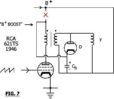
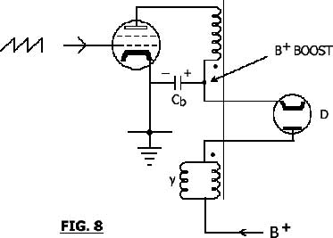
This gives a larger primary supply potential, the B+ Boost voltage, which helps attain the required picture width from a smaller B+. It should be pointed out that, as is always the case, no additional energy is created that was not already supplied by the power supply in the first place. The circuit is simply more efficient because overall, the damped current is not primarily wasted as heat, which it is in all cases of resistive damping. One definition of a resistance is an energy wasting or heat dissipative device. Moving on the Fig 8, we can see what happens if we simply re-draw the above circuit with Cb connected to ground.
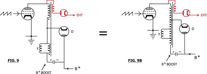
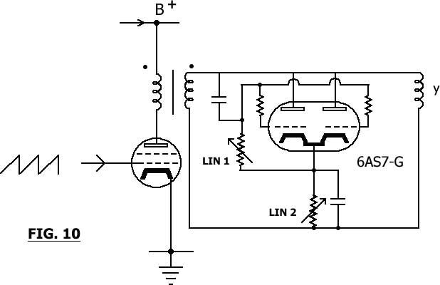
It is a small modification to introduce B+ directly at the anode of the damper diode and then the circuit comprising the secondary, damper diode and Cb can be rotated around to create the circuit of Fig 9 below. The circuit of Fig 9 has the advantage that the Cb only needs to be rated to handle the Boost component of the total "B+Boost" voltage, rather than the total amount. Also the primary and secondary can be one tapped winding, with the yoke coupled across any part of it, in an efficient autotransformer configuration. Admiral used this basic configuration in the early 1950's, for example in their series 23 chassis. In general, by the time efficient energy recovery line output stages had arrived, it had become the custom, as it is in the 621TS, to derive the EHT from an over-wind linked to the plate circuit of the line output tube shown in red in Fig 9, and the heater supply for this EHT diode derived from a small number of well insulated turns on the output transformer. Other variations of damper diode circuits which have occurred in the post war period include a triode pair used as a controlled damper diode, which gives additional control over the linearity of the saw-tooth scanning current. See fig 10 below:
LINEARITY AND DEFLECTION OUTPUT STAGE CIRCUIT DESIGN In general, in the line output stage, every effort is made to keep the resistances of the yoke and output transformer windings as low as possible. In the case of transistor output stages (as shown in fig 5), where the working impedances are lower (lower ratio if dynamic voltages to dynamic currents), the nature of the line output transformer is such that the inductance dominates and the resistances of the coils are very low. This enables the output stage to operate as a saturated switch. The transistor is driven with a step function, or rectangular wave, to cause it to switch on for 2/3 or more of the active scan time leading to the right side of the raster. The rise in current in the yoke when the transistor is switched on is linear because the rate of change of current dI/dt is close to a constant for a period after the voltage is initially applied. The fundamental differential equation for an inductor is V = -L.dI/dt, or voltage equals a constant (the inductance L) multiplied by the rate of change of current with time. So if a rectangular voltage is applied to an inductor, the initial rise in current is a saw-tooth, ideal for scanning. The negative sign in the equation indicates that the emf of inductance, is reactive to, or opposes the applied emf. Of course the current cannot rise linearly indefinitely in an RL circuit, either it will become non linear as the transformer core starts to saturate, or exponentially taper off to a value given by the applied voltage divided by the resistance. The proportions of inductance, applied voltage and winding resistances are chosen so over the time interval of the scan when, the transistor is turned on, the rise in current is substantially linear. At the end of scan, the transistor switched off and the magnetic field collapses for a half cycle of operation, this then forces the semiconductor damper diode into conduction, where it effectively acts like a switch and results in a substantially linear scan on the left hand side of the raster. The transistor line output circuit, however, is therefore such that the transistor, acting as a switch, is very efficient, but the transistor, and its drive waveform can have little effect over the linearity of the scan it generates (unlike a tube line output stage as will be explained). To gain linearity control, in the transistor line output stage, usually a capacitor is inserted in series with the yoke (sometimes called an S correction capacitor), or an inductance in apposition to a permanent magnet is placed in series with the yoke. In contrast the impedances in a tube line output stage (ratios of dynamic voltages to dynamic currents) are higher than in the transistor case. These lower currents (and higher voltages) in the primary circuits require that there are more turns in the output transformer at least, and usually the yoke too. Horizontal yoke winding resistances are in the order of 10 to 60 ohms for tube work, but very low, less than an ohm sometimes in portable transistor TVs with 12-volt supply rails. Overall though, in a tube set, the line yoke coils are transformed to the anode of the line output tube as a substantially inductive load, and the anode voltage wave, with the saw-tooth grid drive is substantially rectangular in character. However, in the case of the tube line output stage, the nature of the grid drive (horizontal drive), unlike the transistor case, is able to influence the linearity, especially on the middle right hand side of the raster. (The line yoke can also be driven directly from the tube anode; in this case the yoke has a higher inductance and higher resistance than in the transformer coupled case) In general linearity controls in tube line output stages are introduced as an inductor in series with the B+ boost supply to the primary winding, with varying amounts of capacitive filtering around this for the B+ boost voltage. The ripple voltage generated alters the output tube's working load and variations in linearity can be obtained that way, which tends to vary the linearity near the picture centre. In contrast, due to the much lower working frequency in the frame circuits, transformers with larger inductances (and also resistances) are required and the load presented to the vertical output tube is a combination resistive and inductive. This requires an overall drive voltage which is a combination of a rectangular wave and saw-tooth (trapezoid) to generate a saw-tooth current is a circuit with series elements of L and R. The design of tube or transistor vertical output stages very much resembles their audio output stage counterparts, and the exact shape of the trapezoidal waveform and the operating conditions of the output device, has a substantial effect on the vertical linearity. This is why one common form of linearity control in a vertical output stage consists of a variable resistor in the cathode of the vertical output tube. Dr Hugo Holden Australia, November 2006.
|